Navid Mir
I am an electrical and computer engineering MS student at the University of California, Los Angeles. My focus is on circuits and embedded systems, and I am interested in all things hardware/software. I hold a BS in electrical engineering from the University of California, Santa Barbara. I have dedicated this website to showcase the different projects I have completed. Enjoy!
Machine Learning Hardware Accelerator
Hardware Accelerator for Image Classification Machine Learning Algorithm
This two-person class project was an RTL implementation of a neural network to perform number classification from images. The MNIST dataset was used to train the model. After the RTL was written in Verilog, we performed synthesis using Synopsys Design Compiler and we verified our design with ModelSim gate-level simulations. We spent the remaining time optimizing the design for minimum power and area and performed word-length simulation
Hylev
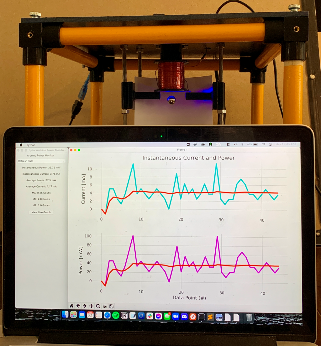
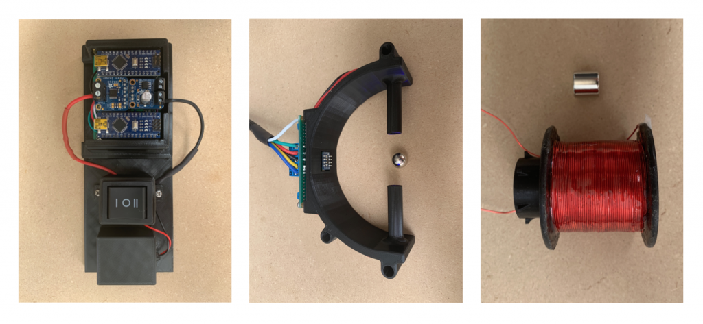
Testing and Research Platform for Ultra Low-Power Magnetic Levitation
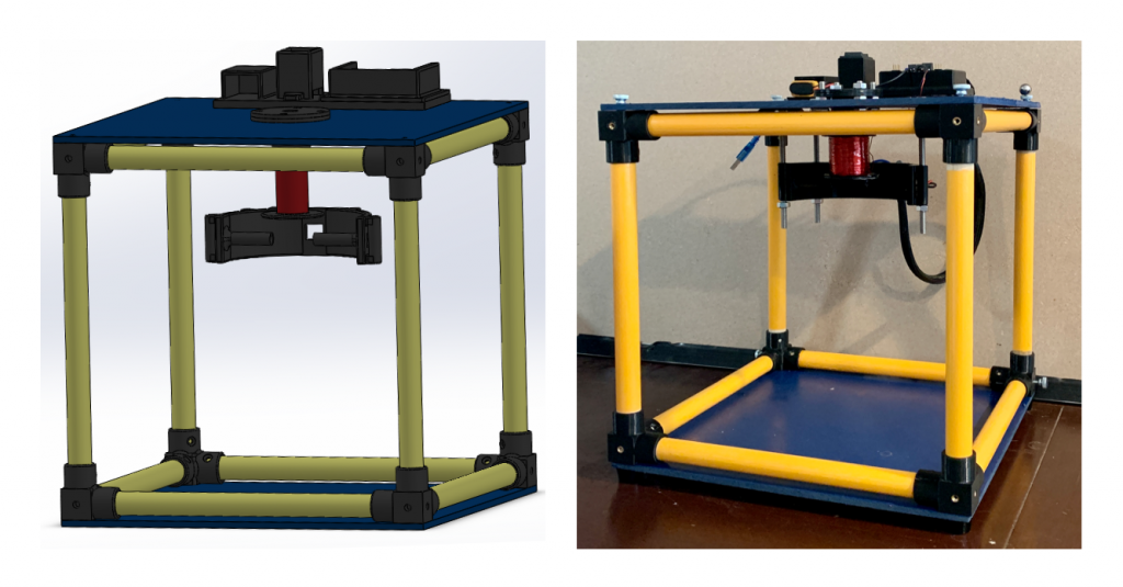
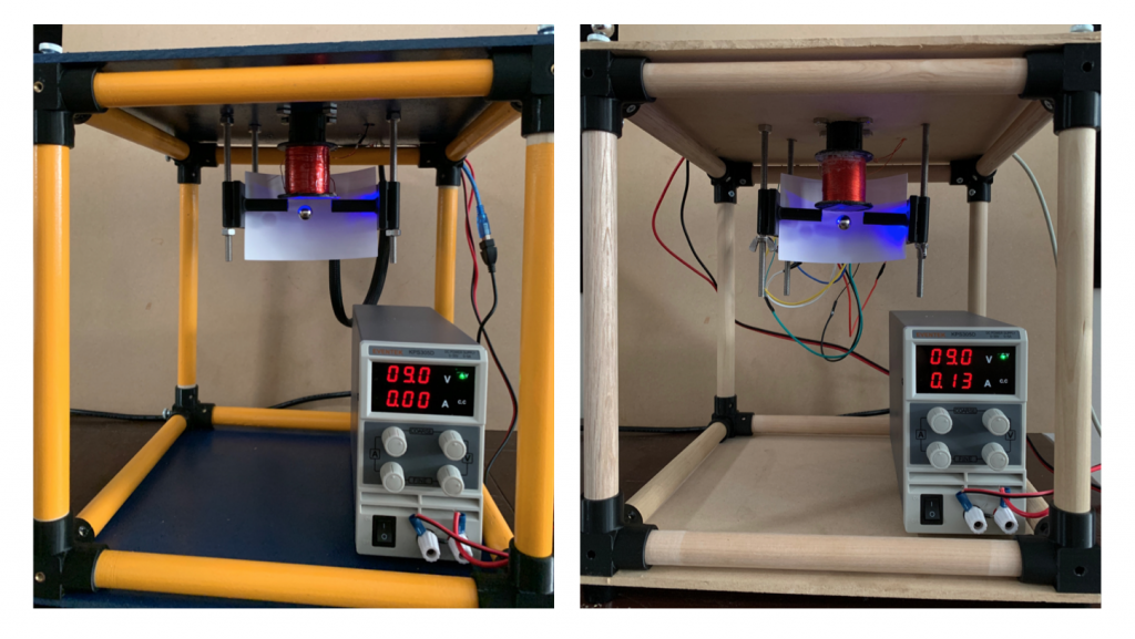
This senior EE capstone project was the design of a testing and research platform for ultra low-power magnetic levitation. Our design uses a hyrbid levitator consisting of a coil and permanent magnet to cut the power over coil-only designs by over 97%! My role was in the control system design (built on Arduino) and coil design/manufacturing, among others. Our project won the top prize in EE: Excellence in Electrical Engineering!
100u x 20u NMOS IC Design
Design of digital and analog circuits with 100u x 20u NMOS
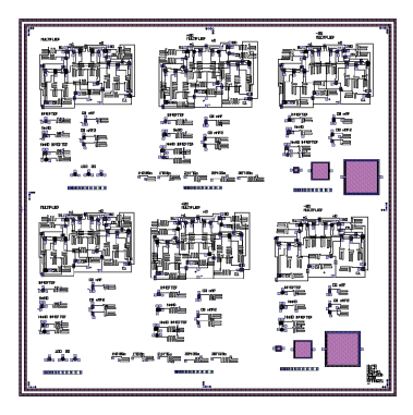
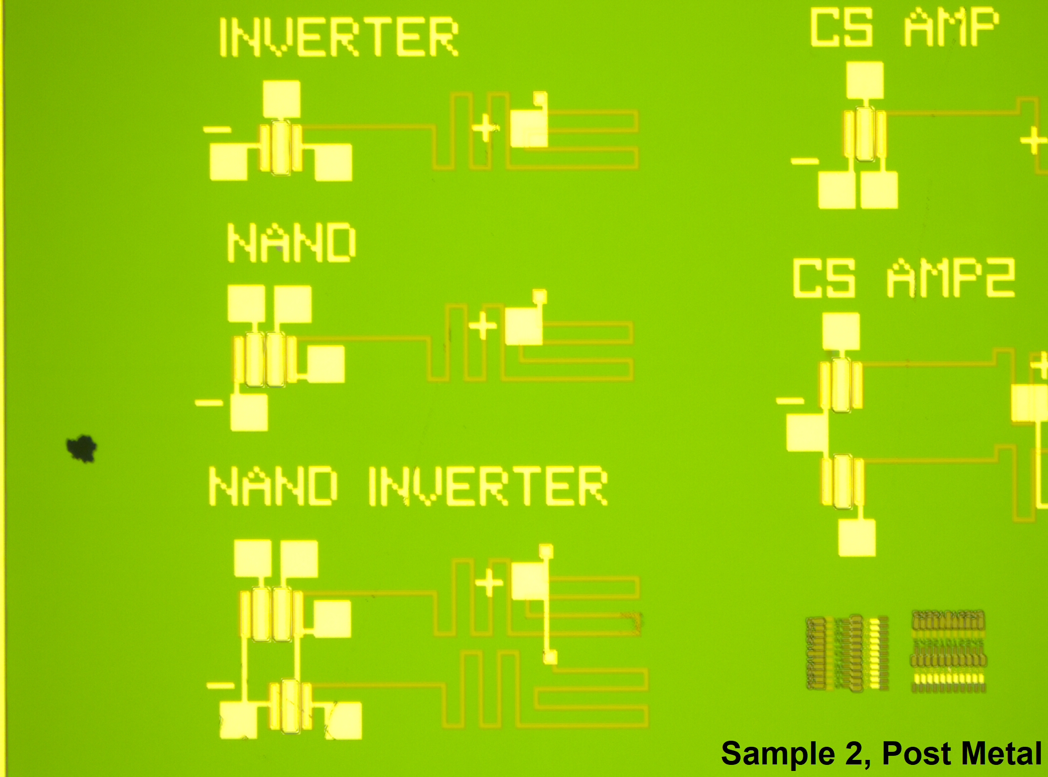
This group project was to design circuits with UCSB's teaching clean room NMOS process. Our group design a 2 by 2 binary multiplier, NAND gates, digital inverters, and common source amplifiers to be fabricated with 100u x 20u NMOS transistors. We designed the masks which were fabricated by the California NanoSystems Institute on campus. We then went through the four layer fabrication process in the clean room to fabricate the circuits.

Virtual Piano Teacher App
Android Piano Note Visualizer Application using FFT
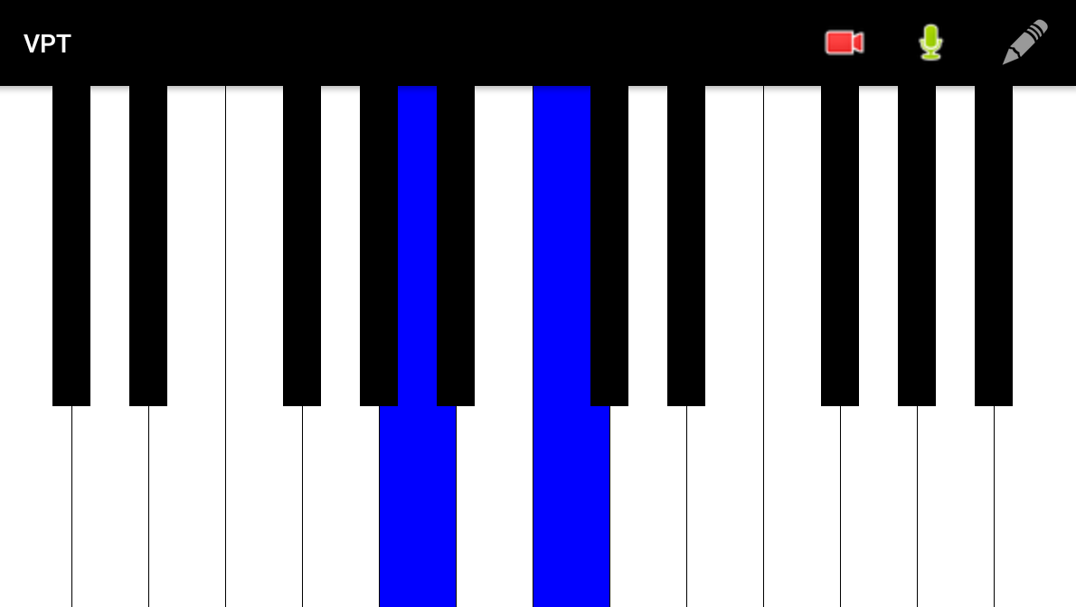
This solo project is an Android application written in Java that enables users to sample their piano playing and display the played notes on a piano GUI. The application uses the Fast-Fourier Transform (FFT) algorithm to produce the spectrum of the notes played to extract the frequency content of the sampled audio. The spectrum is then processed and the frequency components present are mapped to the key frequencies of a piano to display the notes played. The user can then record the piano GUI screen and save it. This application can be used by students who want to verify their note accuracy or piano teachers who want to record lessons for their students.
MOSFET Fabrication
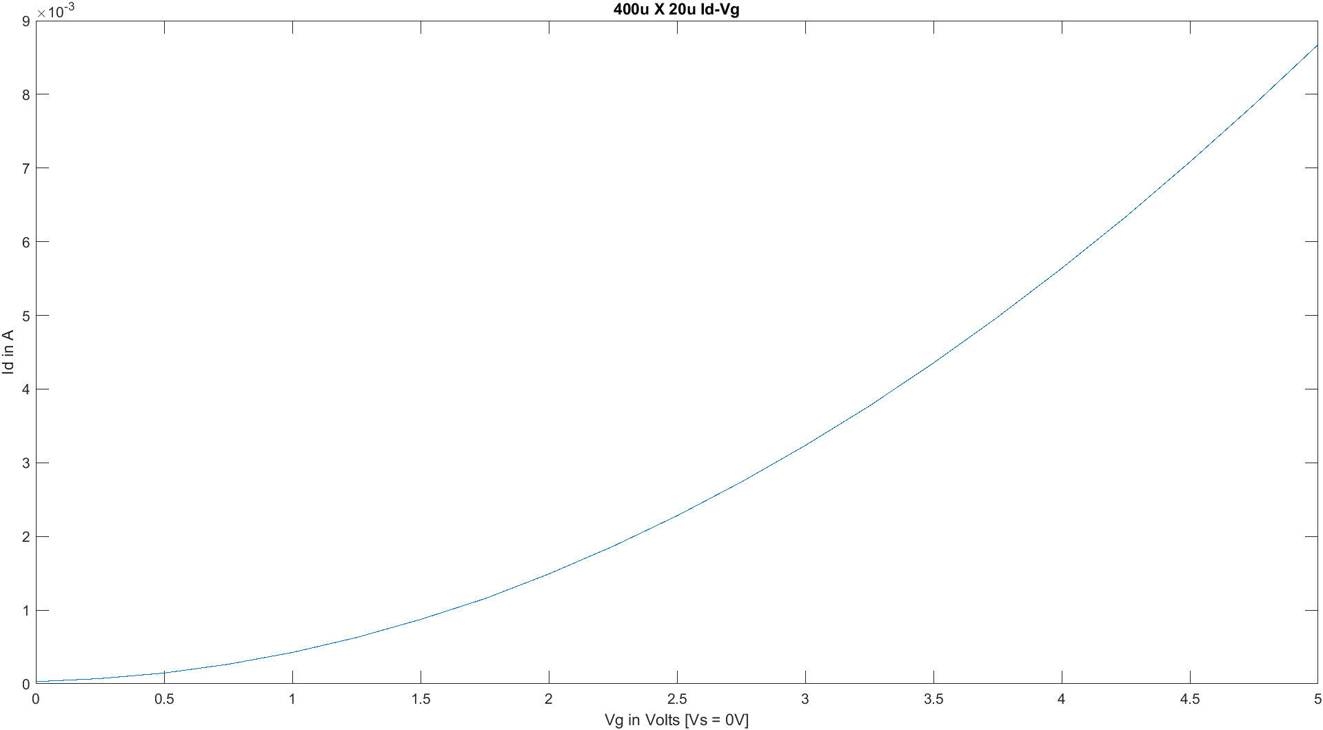
Fabrication of n-Channel MOSFET from bare Silicon
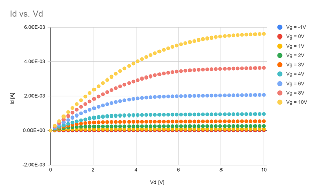
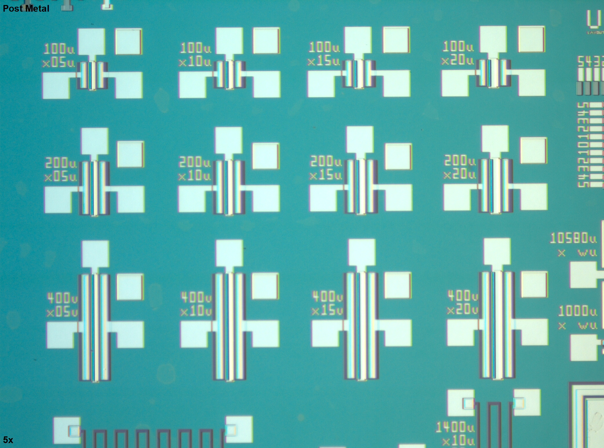
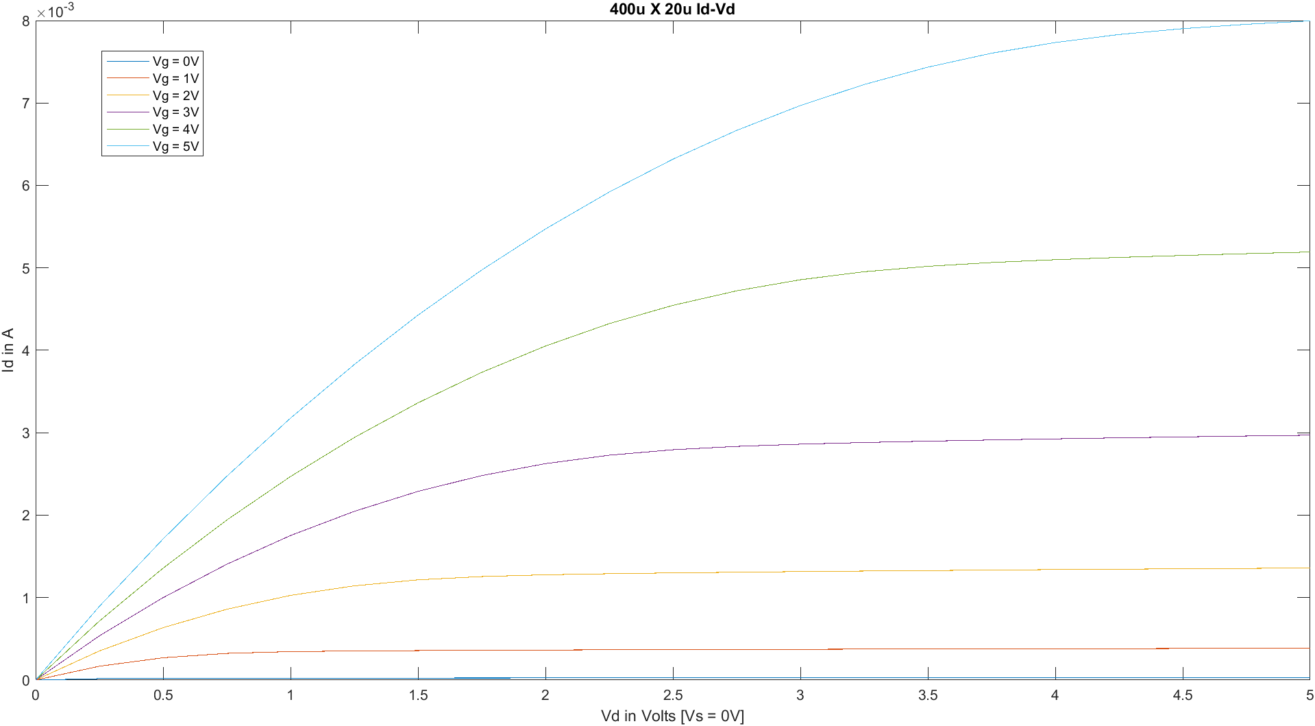
This group lab project was to fabricate an n-MOSFET (n-Channel Metal-Oxide Semiconductor, Field Effect Transistor). Starting with bare, p-type doped Silicon wafers, we layered our samples with 4 total Masks. We used photolithography with a mask contact aligner to expose the photoresist on our samples and developed them in a base developer. We grew silicon dioxide for three different functions, one for the field, one to drive in our phosphorus n-type dopants for the source and drain regions, and one for the gate. We doped these souce and drain regions with phosphorus by first performing predeposition, and then performing a drive-in of the dopants with an oxide growth. To etch the oxide, we did wet-etching with hydrofluoric acid. Our last steps were to do aluminum deposition on the wafer with electron-beam evaporation and to perform liftoff to reveal our working transistors! The gate dimensions of the devices are from 100μm X 5μm to 400μm X 20μm.
Plasma Speaker
High-Voltage Plasma Arc Speaker
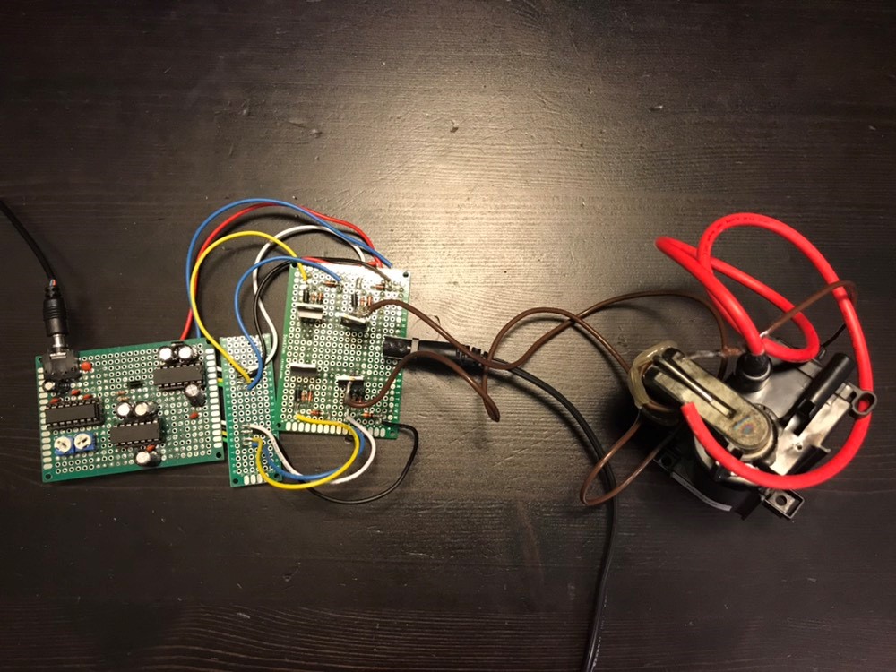
This project allowed for a music signal from any standard device to be played by a high-voltage plasma arc. I assembled three different circuits. The first circuit generates a PWM signal from the MIDI audio input. This PWM signal is then amplified in the second circuit. The final circuit, a MOSFET H-bridge, then converts the amplified DC signal to AC to allow for a transformer to step up the signal voltage and produce the arc at the corresponding music frequencies.
openSesame
Facial Recognition Smart-Lock
This project uses OpenCV (Python Computer Vision Library) to match allowed users and automatically open a lock to a house or room, allowing key-less entry. This project was a submission to the SB Hacks V Hackathon at UC Santa Barbara where my team won the Best Security Hack Award sponsored by Arthrex, Inc. Users start by uploading a single image of each person allowed to enter on our website hosted on the Google Cloud Platform. When a guest wants to enter, they have a picture taken at the door which is then sent to our server that uses a machine learning computer vision algorithm to determine if the guest is a match with the allowed guests. The server then sends a response to a Raspberry Pi located at the door. The Raspberry Pi interprets this response and then sends it to an Arduino which then can operate a servo that locks/unlocks the door and displays messages to the guests about their status. I designed and put together hardware and worked on software integration. Specifically, I made a Raspberry Pi circuit that runs JavaScript code to access our server on the Google Cloud Platform for a facial recognition program response. The Raspberry Pi then converts the response to a digital signal to have an Arduino turn a lock using servo motors and display messages on an LCD.

Github Repository
Devpost Submission
LED Tetris
32 x 32 LED Panel Tetris Game Console
This project allows users to play Tetris on a vibrant LED panel. I wrote the Tetris game code on an Arduino Mega, which interfaces with the LED panel via a library that controls each LED individually. I also integrated a joystick to give an arcade-style feel to the user.
LED Cube Display
4 x 4 x 4 LED Cube Light Display
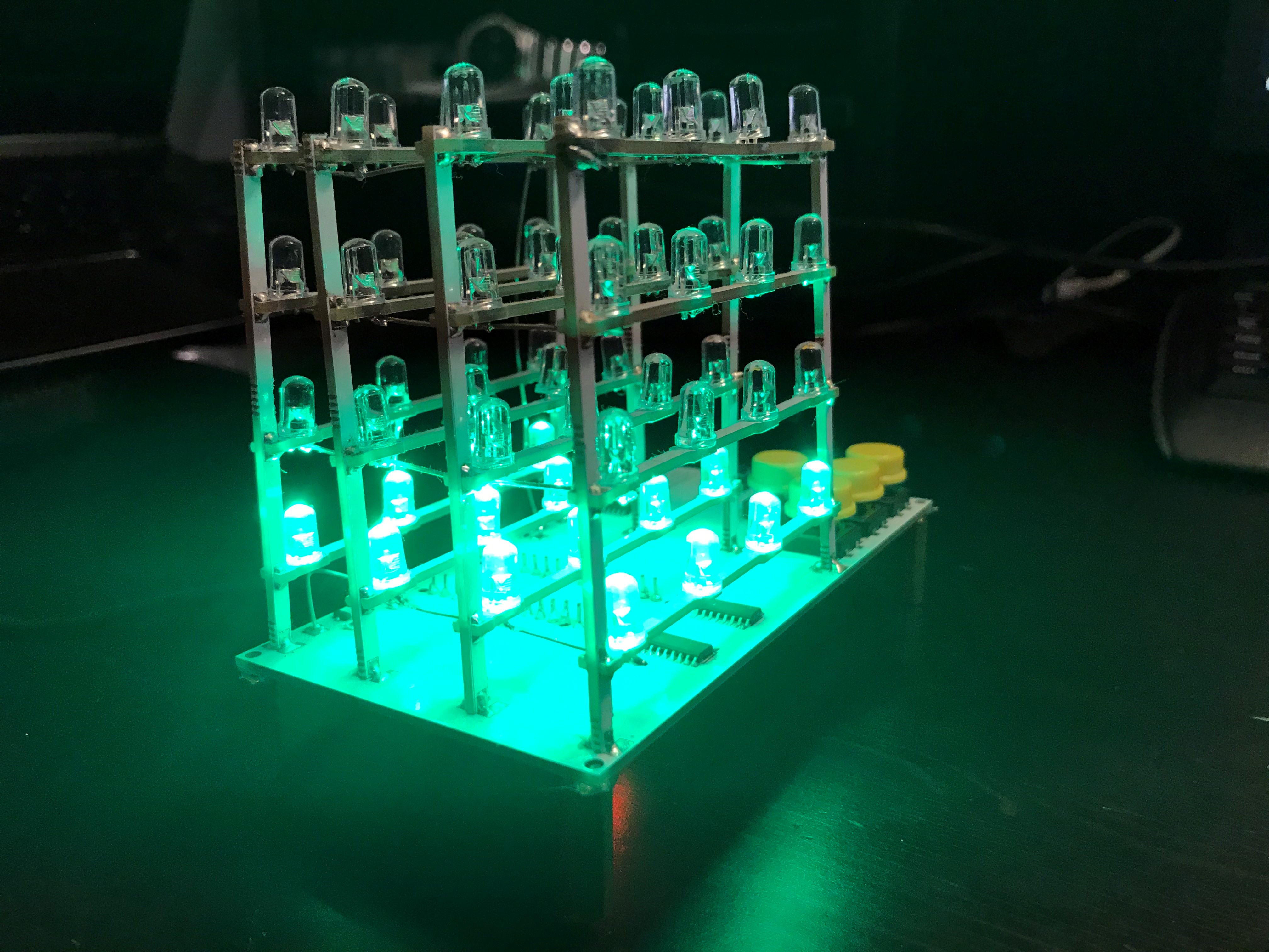
This project allows for 3D designs to be displayed on a 4 by 4 by 4 cube of LEDs. I constructed the LED cube and circuitry and wrote microcontroller code on an Arduino Nano for the designs.
Machined Lightsaber
Machined Aluminum Lightsaber Hilt
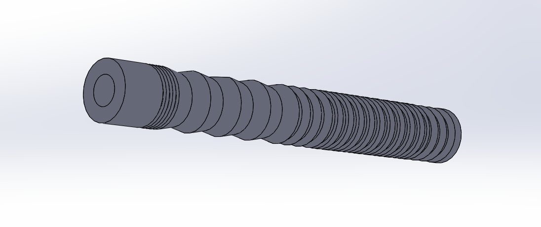
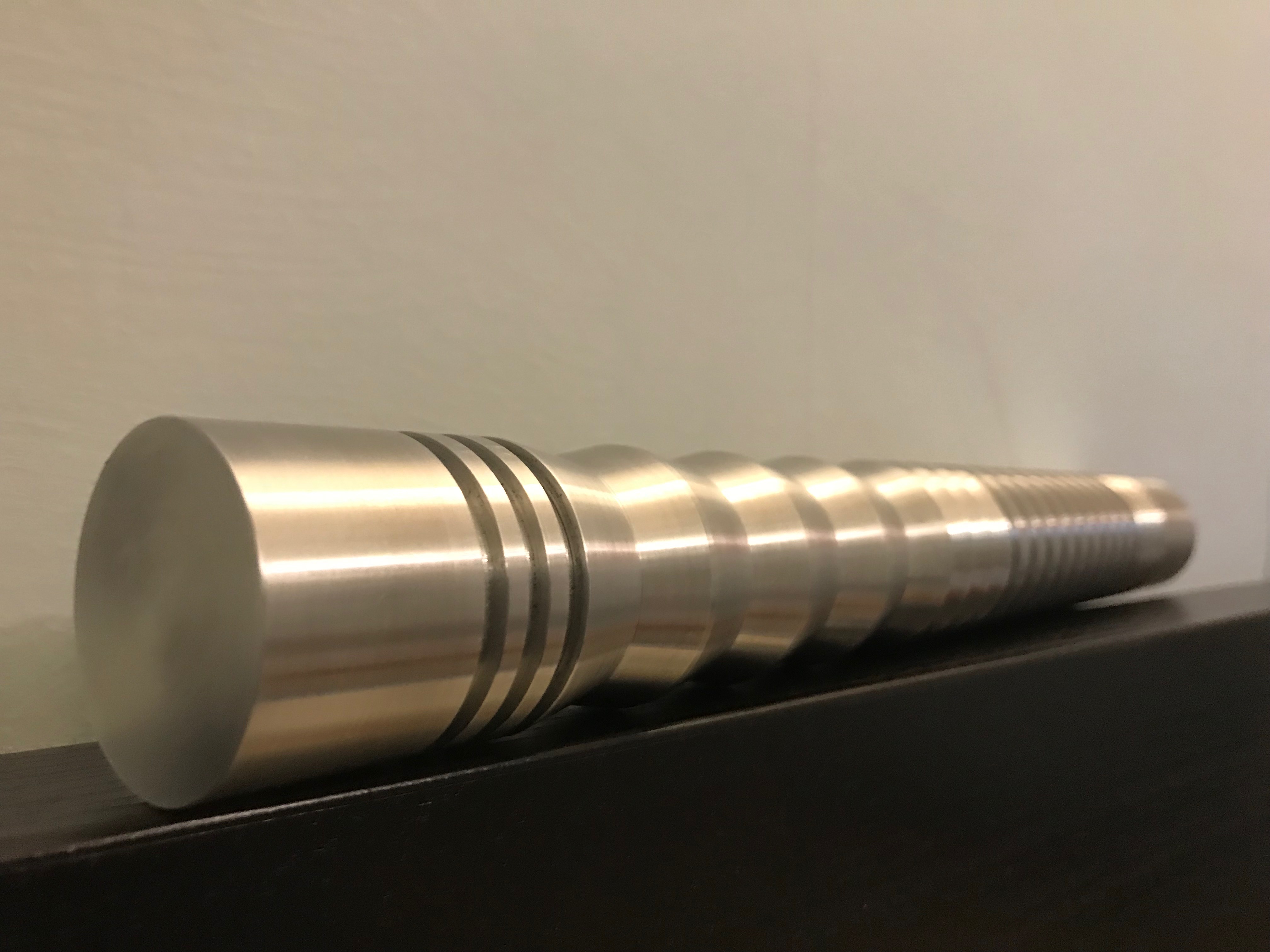
I created a lightsaber with a machined aluminum handle through the UC Santa Barbara Machine Shop Club. I designed CAD specifications of the handle from scratch using SolidWorks. I then made the handle by lathing aluminum stock based off of the specifications of my CAD design.